

The internet-of-things revolution is here and it is here to stay. From internet-enabled cat boxes to Wi-Fi-controlled stoves, smart devices permeate our lives at an ever-increasing increasing pace. The rush to get items like the next greatest internet-connected wine bottle to market coupled with the lack of regulatory oversight frequently puts system security on the back burner; a feature to be “added on later.” Rather than focus on product security, many manufacturers and integrators choose instead to disable hardware debugging functionality and enable firmware readback protection to make vulnerability discovery more challenging.
Once these microcontroller interfaces are locked, there is usually no manufacturer-prescribed way to unlock them without also wiping out the firmware. Historically, there have been ways to bypass these lockouts, often because the manufacturer doesn’t realize how attackers can abuse certain functionality. For instance, manufacturers sometimes unwittingly allow readback of firmware through faulty implementations of the hashing algorithms used to validate flashing at the factory. If a debugging interface is available, researchers can sometimes extract the firmware through side-effect analysis. There are more involved attacks such as voltage or clock glitching using toolkits, like the venerable ChipWhisperer, that inject faults to try to trip up internal subsystem behavior during critical operations.
Another class of attacks, referred to as invasive,” requires physical access to the silicon dies inside of the package while maintaining chip functionality. These are often dismissed as infeasible for the average security researcher due to the perceived difficulty and expense of IC decapsulation. The goal of this guide is to demonstrate that researchers don’t need a multi-million dollar lab to perform practical invasive attacks against a typical microcontroller and to detail a novel method of utilizing safer acid mixtures at or below room temperature to decapsulate semiconductor packages that utilize copper interconnects and wires. At the end, I will cover common mitigations employed and how to spot them.
At their most basic, we can think of hardware configuration flags that allow access to debug interfaces and firmware readout as wires burned into an open circuit. However, manufacturers implement this in many different ways at the silicon level. While eFuses and antifuses do behave in essentially this way by permanently breaking down some conductive or dielectric layers, these are rare in the MCU world; we typically find them in Complex Programmable Logic Devices (CPLDs) and, most notably, Microsoft Corp.’s Xbox 360’s CPU. More often than not, there is a logically (and often physically) isolated area of common flash memory that holds these control bits without providing an external means of resetting them once set. Flash memory itself is based on a type of transistor discovered in the 1960s called a floating-gate transistor. These transistors are special in that they can trap and hold charge for long periods. The simplest type of array of floating-gate transistors is called Erasable Programmable Read Only Memory, or EPROM for short.
By default, these floating-gate transistors are at a logic high. When a logical low needs to be stored, the control gate is energized by a high programming voltage (VPP in most datasheets) and electrons become trapped in the electrically-insulated floating gate directly below through a quantum tunneling process called hot-carrier injection. This charge-implantation process changes the electrical characteristics of the transistor. These characteristics can be measured by applying a lower read voltage to the control gate and sensing if the current passes through the transistor, effectively storing a single bit of information.
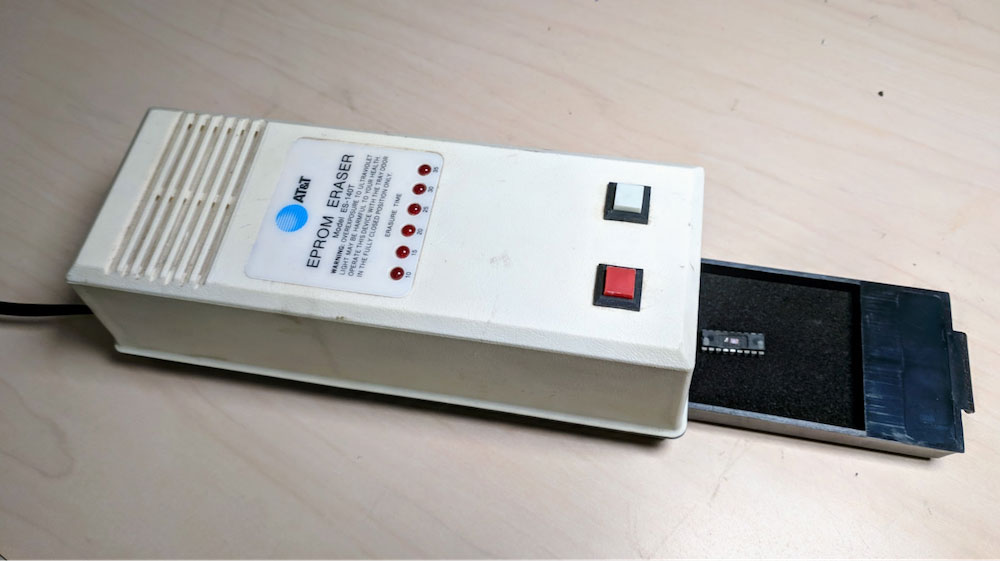
These simple EPROMs have a significant limitation: if the cell needs to be updated and reset to a logic-high state, the charge stored in the floating gate needs to be cleared. The primary method for knocking this latent charge out of the floating gate used high-energy photons from a glorified ultraviolet (UV) flashlight called an EPROM eraser. This is why old EPROM packages have quartz windows topped with adhesive stickers protecting them from accidental erasure due to errant UV sources like the sun.
This inability to electrically reprogram EPROMs led to the development of the EEPROM, or Electrically Erasable PROM, which utilizes an additional quantum tunneling effect (Fowler–Nordheim tunneling) to also electrically drain the charge from the floating gate. Modern flash memory adds a charge pump to create the high programming voltages internal to the circuit and clusters these cells so they can be erased— or “‘flashed”’ off— together.
While all these ancillary functions are new, ultimately modern flash memory is still based on the same floating-gate technology as the EPROM. This means that if I expose the floating gate to enough UV light, I can alter its value.


Before we get ahead of ourselves, it is important to understand the structure of a typical electronic component package. I’ll be primarily focusing on a standard single-die DIP (dual in-line) package, but the methodology and techniques are nearly identical for other types.
What we commonly think of as pins are not actually directly connected to the silicon die. Instead, the pins form a lattice surrounding the die, often referred to as a lead frame and are typically made of either aluminum or aluminized copper. In the center of this lead frame is a paddle that acts as a mechanical support for the silicon die placed atop it.
Each lead of this lattice is then ultrasonically welded to the silicon die by a 0.003-inch to 0.020-inch thick bonding wire. Manufacturers historically used gold for these bond wires, but now more frequently use copper due to its lower cost and superior electrical characteristics.
One of the major challenges in performing live target analysis on the cheap is keeping these incredibly fragile bond wires intact throughout the decapsulation process. While it is possible to repair broken bond wires, their scale requires expensive, industrial wire-bonding stations, so decapsulation methods should keep this delicacy in mind and avoid bond wire damage.
Once the bond wires are attached between the lead frame and the silicon die, the entire arrangement is placed into an injection molding machine and surrounded with Epoxy Molding Compound (EMC). This compound is typically only 5 percent to 20 percent actual epoxy resin, as the resin has a high degree of thermal expansion that could break bond wires or cause internal stresses that can fracture the die. The majority (60 percent to 80 percent) of the molding compound is silica or alumina filler to compensate for the thermal expansion. The rest is usually a proprietary blend of rubbers, dyes and plastic softeners. The ultimate goal of the various decapsulation methods, when applied to live-target analysis, is to delicately remove this molding compound above the die without damaging it or the surrounding bond wires.

Throughout this process I will have to destroy several chips. Unless the target is relatively inexpensive, heading over to a favorite component peddler like DigiKey or Mouser and ordering a fist full of spares is a wise idea. I’ll use them to take measurements, run experiments and refine the overall decapsulation and firmware extraction process. Chemical wet etching, like what I will be doing later, can be a slow and expensive process in terms of reagents consumed. That’s why it is important to leave only the bare minimum of work for the acids and to remove the majority of the molding compound by other means.
Before I remove any material, I need to know where and how much of it to remove and the easiest way to accomplish that is with a belt grinder and a flatbed scanner. I start by clipping off all the leads from one of the sacrificial chips and begin to sand away material from the side of the package where the leads once were.
I’m interested in simply removing bulk material, so I use a coarse-grit sanding belt to progressively sand the edge down. I try to keep it level, but it doesn’t need to be perfect. As grinding progresses, the lead frame fades away and eventually the edge of the silver-colored die itself sitting on a bit of copper becomes visible. Once I hit this point, I stop sanding, clean it with isopropyl alcohol, throw it on my flatbed scanner and scan it at the highest DPI setting. Once scanned, I’m greeted with an image like this:
Here I can make out all the components of the package. Most importantly, just above the die, I will see a series of small metallic speckles, which are the bond wires coming in from the lead frame and approaching the die. This is my first glimpse of the scale, material composition and fragility of these wires. From this image, I measure:: the width of the die itself, the offset of the die from the “front” and “back” of the package and the depth of the bond wires as they approach the die. The latter will be the target depth of the material removal, minus a small fudge factor.
Now I can finally go on to removing just the right amount of molding compound. The semiconductor failure analysis industry typically uses a laser ablative process for this step, but utilizes expensive high-speed galvos to rapidly scan the beam. While compound removal is possible with a standard plotter-style laser cutter, it is likely to produce a ridged surface that will etch unevenly and damage the chip in the process. Preferably, I would use an inexpensive PCB mill, but thanks to the scale, even a 3D printer with a Dremel strapped to the side will do.
In my case I printed a Dremel flex-shaft holder for my Lulzbot TAZ 6, attached an aquarium pump to blow off the removed material and modified some firmware parameters to get homing and leveling working properly. To hold the chip in place during the milling operation, I soldered a DIP socket to some perf-board and stuck it down to the build plate with some painters tape.
Using the cross section image captured earlier, I created a 3D model of the package. I prefer Fusion 360, but any CAD package will suffice. In the model, I created an elongated well going down to—but not touching—the bond wires. How close really depends on the repeatability of one’s process but I shoot for less than 0.1 millimeter. The closer I can get, the faster the etching will go. I also like to add a pair 0.5 millimeter deep holes on opposing sides of the chip that I can place a depth gauge in to determine how (not) level my build plate is and whether I’m cutting to the depth that I intended. I also add a chamfer to the pocket so that the die can be UV-exposed at an angle if necessary.
To machine the cavity, I use inexpensive 1.0 millimeter end mills and generate the tool paths accordingly. I then place the chip into the DIP socket and execute the G-code that controls the milling device. A truly repeatable setup would allow for progressively increasing the cutting depth and testing chip functionality between passes to get as close to the bond wires as possible.


In high concentrations, nitric acid is some pretty scary stuff. Even in moderate concentrations it will release poisonous nitrogen oxide gases (NOx) that will kill you. It is of paramount importance to perform the etching in a well-ventilated area with appropriate personal protection equipment.
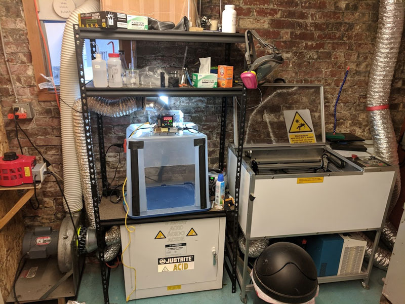
Most etching procedures call for the handling of large volumes of extremely expensive and reactive fuming nitric acid and holding it close to its boiling point (83 degrees Celsius). The methodology covered here uses a chemical process to concentrate small volumes of more dilute nitric acid to its fuming counterpart at or below room temperature making the procedure much safer due to the reduced reactivity and fuming at the cost of increased reaction run-time. The following protections should be considered the absolute bare minimum requirements and are unique to the considerations of my lab. Additional safeguards may be necessary and implementing the right ones requires expertise, research and planning.
Inexpensive acid-safe fume hoods are available from overseas sellers or from surplus suppliers at local universities and on Craigslist. To keep costs down, I built my own. When designing an enclosure, it is important to consider material reactivity with the chemicals involved. I settled on two of the largest polypropylene containers from my local Home Depot. One donated a large portion of its side to become a sliding sash while the other became the hood body. A three-way outdoor power splitter and a 4-inch starting collar were siliconed in place.
While this is far from ideal fume hood geometry due to its lack of back baffles and front air foils as well as its being being made out of a Sterilite box, it functions perfectly well through the application of brute suction force. Attached to it through a series of HVAC hoses and mating plates is a single horsepower industrial blower motor that can pull 500 cubic feet of air per minute.
This is a ridiculous amount of airflow, but it was what I had on hand. I ended up adding a type of variable transformer called a Variac to control its speed. There are less expensive and better-suited blower fans available online with built-in speed controllers. To test the fume hood, I used a high-volume party smoke machine to make sure air was flowing inward by moving it around the entire perimeter of the hood. I then placed the smoke machine nozzle inside the hood and verified the absence of vortices that could direct fumes outside of the hood.


While no respirator without an external air supply can filter out NOx fumes, there are plenty that will filter out sulfuric and side-reaction fumes. After familiarizing myself with types of respirators, I purchased a full-face respirator and an appropriate filter cartridge.
When dealing with fuming nitric acid, even in tiny quantities, nitrile or latex lab gloves will simply not suffice. Viton is a synthetic rubber that is highly resistant to nitric acid attack and is used extensively in the petrochemical industry for O-rings and gaskets. Luckily, one can also purchase Viton-coated butyl gloves.
Of note is that these gloves are sensitive to acetone, which can make them tacky. One should not rely on gloves protecting them, they are there only as a backup. I tend to wear a pair of nitrile gloves under the Viton gloves to make the outer gloves easier to take on and off repeatedly.
A lab coat, meanwhile, isn’t just for costume parties; it’s an invaluable protective layer separating you from a really bad time if something goes wrong. When choosing a lab coat, I look for thick, natural fibers that will take time to soak through. Buttons take time to undo so I try to pick one with snaps that I can remove quickly.


The most important thing to have is a plan. I try to ask myself what can go wrong at every step and what I can do to mitigate those risks. If my exhaust fan dies, what am I going to do? If a fire starts do I have an appropriate means to extinguish it? Where will I put acid-contaminated tools and pipettes? If I have an acid spill, how will it be contained and neutralized? Can I get to an eyewash station while blind? If something happens to me, can someone help me without endangering themselves? Have I understood the Safety Data Sheet (SDS) for each of the chemicals I am using and are they on hand?
What actually happens during nitric acid wet etch of epoxy molding compound? Nitric acid typically acts in three distinct ways: As a proton donor, a strong oxidizing agent and as a nitrating agent. When it comes into contact with the molding compound, nitric acid oxidizes the resin hardener within, causing the epoxy to break up and release the silica filler. However, dilute nitric acid also reacts with copper to produce copper oxide and copper nitrates which are soluble in water, effectively dissolving the metal. Due to a spike in the price of gold and superior electrical characteristics of copper, the semiconductor industry has been steadily shifting from gold bond wires to copper.
To keep delicate copper bond wires from dissolving, the failure analysis industry uses temperature-controlled and highly concentrated (>98 percent) white fuming nitric acid (WFNA), with a small amount of concentrated sulfuric acid added. While the WFNA reacts with the copper metal to produce NOx gases, water, copper oxide, and copper (II) nitrate, the concentrated sulfuric acid acts as a dehydrating agent, keeping the copper (II) nitrate from becoming soluble. It quickly forms a protective crust around the copper metal preventing further acid attack. This is done while holding the reaction mixture at a lowered (10 Celsius) temperature to slow the normally vigorous reaction. Fuming nitric acid can be used by itself to achieve this, but as it reacts, more water is generated, increasing solubility over time and wearing away the protective nitrate coating, further eroding the bond wires. This property of concentrated nitric acid as it reacts to copper is called copper passivation.
Fuming nitric acid is an extremely dangerous chemical to make, transport, store and use. This makes it fairly difficult to obtain and comes at great expense (around$400 delivered via special commercial carrier per half liter) and even so only after chemical supplier authorization which can be a lengthy and cumbersome process. Distilling concentrated nitric acid into its fuming variant is stymied by the formation of what’s called an azeotrope with water— the two become inseparable through fractional distillation at a concentration of 70 percent.
Independently synthesizing fuming nitric acid, while possible, is extremely dangerous as it involves distilling nitrate salts with sulfuric acid. After many experiments and countless failures, what I have developed is a process using concentrated 70-percent nitric acid which is readily available, safer to store and can be shipped by U.S. carriers to residential addresses for about a tenth the price of fuming nitric acid. The ultimate goal of the industrial preparation is to have a low water content relative to the nitric acid to achieve copper passivation by utilizing the concentrated fuming variant and taking care of the water generated in the reaction through concentrated sulfuric acid drying.
By having a large excess of concentrated 98-percent sulfuric acid relative to the dilute 70 percent nitric acid, I can bind the water present in the nitric acid and reduce solubility of the copper (II) nitrate layer protecting the bond wires. This allows me to oxidize the molding compound away, while leaving the chip functional in its original package. As an added benefit, the amount of sulfuric acid added can moderate the reaction rate sufficiently to achieve copper passivation and effective molding compound etching at room-temperature, requiring no external heating or cooling albeit at the cost of increased reaction run-time. The target mixture that I have found to work best for samples is a 2:1 ratio (by volume) of 98 percent sulfuric acid to 70 percent nitric acid. I typically prepare only 3 milliliters to 6 milliliters of the mixed solution at a time to keep reagent waste low, preparing more as I run out or as all the nitric acid decomposes out of solution.


In addition to the concentrated nitric and sulfuric acid, to perform this procedure I was going to need some basic lab equipment and chemicals. On the glassware side, I needed a variety of Pyrex beakers ranging from 50 milliliters to 250ml, a set of glass Petri dishes, a 5-milliliter graduated cylinder, a watch glass to fit over the beakers, a glass stir-rod and a Pyrex baking dish to catch any spills. Additionally, I needed a pair of squeezable wash bottles, some pH test strips, a bag of disposable 3-milliliter transfer pipettes, a set of tweezers and a stock of canned air. As far as additional chemicals go, all I needed was some hardware-store grade acetone, a jug of distilled water and common sodium bicarbonate (baking soda) from the grocery store.

Outside of the fume hood, I fill one wash bottle with acetone and the other with distilled water. In a large beaker, I dissolve baking soda in tap water until the solution is fully saturated and the soda begins to accumulate on the bottom of the beaker. I add more until I have about a quarter-inch of baking soda collected on the bottom to act as a buffer. This will be my neutralizing solution that I can use to neutralize both acids.
I lay out my fume hood workspace and mark my beakers for what they are to contain.
After putting on my safety equipment, I turn on the fume extractor and retrieve my acid bottles from storage. Using a transfer pipette, I measure out 2 milliliters of nitric acid in a graduated cylinder, pour it into an empty 50-milliliter beaker and cover with a watch glass.
Using a fresh transfer pipette I measure out 4 milliliters of sulfuric acid in a graduated cylinder. Note that concentrated sulfuric acid is much more viscous than the nitric acid. I add this slowly to the beaker with the nitric acid 1 to 2 milliliters at a time. When I add sulfuric acid to the nitric acid, the sulfuric acid will react with the water in the nitric acid in an exothermic manner. It is important to add the sulfuric acid to the nitric acid and not the inverse as there is the risk of flash boiling occurring. I keep an eye on the solution and when I see steam I stop and wait for the solution to cool down. I repeat this process until all the sulfuric acid is mixed in to the nitric acid forming the etchant, or etching solution. Visible wisps of acid fumes will be present and I check on the solution’s temperature with an infrared thermometer.
After covering the etchant with a watch glass, I let it sit until it returns to room temperature, about 10 to 20 minutes.

Finally, I can begin the actual etching process. After placing one or more of my samples in to a Petri dish, I draw a small amount of the prepared etchant in to a transfer pipette and place 4 to 5 drops of it into each milled cavity to fill it. I cover the samples with the other half of the Petri dish and observe.
The reaction is slow to start but the acid should begin to discolor. Eventually, small bubbles of gas will begin forming inside the cavity. If they don’t, I try to adjust the acid ratio slightly to suit the unique characteristics of the particular molding compound or lightly warming the cavity with a hot-air gun.
After 20 to 30 minutes, new bubbles should no longer be forming. Using tweezers, I pick up the package and carefully tap out the acid in to a waste acid beaker, return it to the Petri dish and refill the cavity with fresh etchant. Bubbles will likely be much less vigorous on subsequent etching passes.
After performing this process two or three times—or until the acid appears to have a diminished effect—I fill a 50 milliliter beaker with approximately 15 milliliters of acetone, enough to fully submerge the sample. Using a pair of tweezers, I submerge the entire chip in the acetone and waft it around gently. The aim here is to wash the insoluble silica filler and disintegrated epoxy out of the cavity to expose fresh molding compound to the etchant. It is important to place the sample into the acetone and not acetone into the sample as the acid can react exothermically and build up heat invigorating the reaction and potentially destroying the bond wires.
Silica grit will start to accumulate on the bottom of the acetone beaker. If the bond wires are not yet visible when I lift the sample out of the acetone, I use a squeeze bottle of acetone to gently wash the cavity further. I dump the contents into a larger, uncovered waste acetone beaker and rinse the residue out with fresh acetone.
Before introducing fresh acid, it’s critical that the chip be fully dry of acetone residue. Using a can of compressed air, I gently blow out the cavity until the surface appears dry.
I return the sample to the Petri dish and repeat the process from the beginning with multiple rounds of etching and acetone washing. The number of times I have to repeat this process is dependent on how close I was able to get to the bond wires. If the process stalls and bubbles stop forming or are extremely fine, I use a pipette and blow some air at my acid beaker, if I don’t see any white nitric fume wisps then the majority of my nitric has decomposed and I need to mix a new batch of acid. Eventually, the bond wires will begin to emerge and, after a few more etching passes, the die itself will be revealed.
Once the die is sufficiently exposed, it is time to wash the sample and remove any remaining acid residue. I gently, but thoroughly, rinse the sample with acetone before dunking and wafting the sample in a beaker of distilled water. I decant the water into an acid waste beaker, refill with fresh distilled water and let it sit for 5 minutes while the acid residue is displaced. Periodically, I test the pH of the water wash and repeat the decanting and washing steps until the pH is of the solution is a neutral seven and remains stable for half an hour. Finally, I remove the sample and set it out to dry.
With the package is decapped and the die exposed, it is time to clean up and dispose of all the waste. I begin slowly adding the unreacted etchant into the neutralizing solution. When the two come in to contact, a large amount of gas is generated that will foam up, so I try to go slowly. Once no more gas is being generated, I test the pH and make sure it is still at seven. I repeat this process for my acid waste and wash the pipettes and Petri dish in the solution. After letting the waste acetone evaporate naturally under the fume hood until only a thick sludge is left, I neutralize it as well. I wash all equipment with hot, soapy water and leave to dry. Finally, I wipe down interior work surfaces with a paper towel wetted with the saturated neutralizer.
With the unlocked sample decapped and working, I can start to characterize the internal storage to determine which portion of the die to mask off. Here I will be focusing on the familiar, one-time-programmable, PIC16C54A. Looking at the die under a microscope, I can easily spot the floating-gate transistor array by its relatively large uniform texture surrounded by row and column drivers:
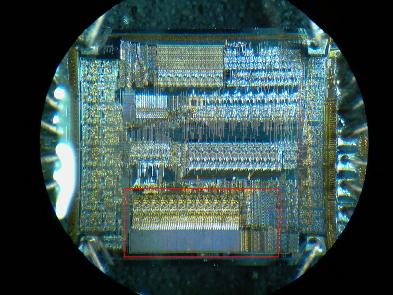
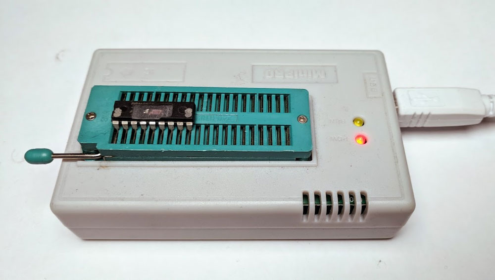
To characterize EPROM storage, I will be programming the device to see if I can alter its contents by exposing the die to UV light. To program and read the contents of this microcontroller, I use a multi-programmer like the MiniPro TL866.
The default state for floating-gate-transistors is at a logic high, so reading the contents of the 12-bit word chip shows pages of 0FFF:
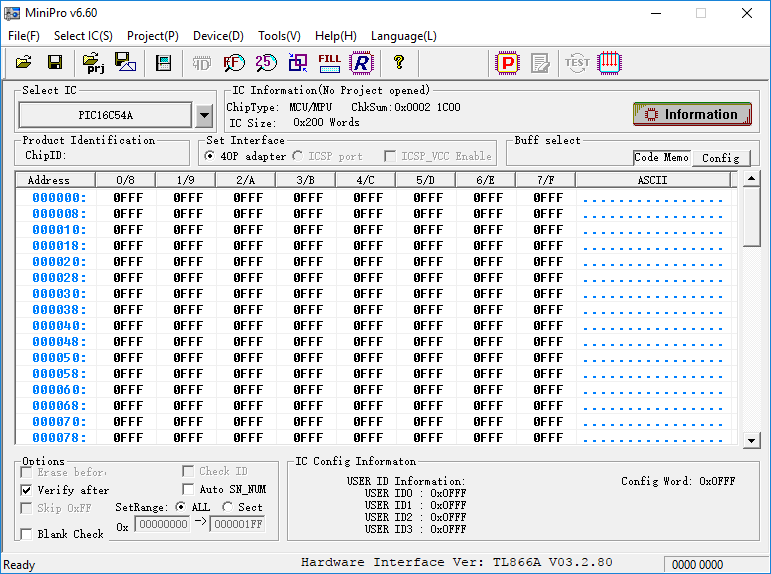
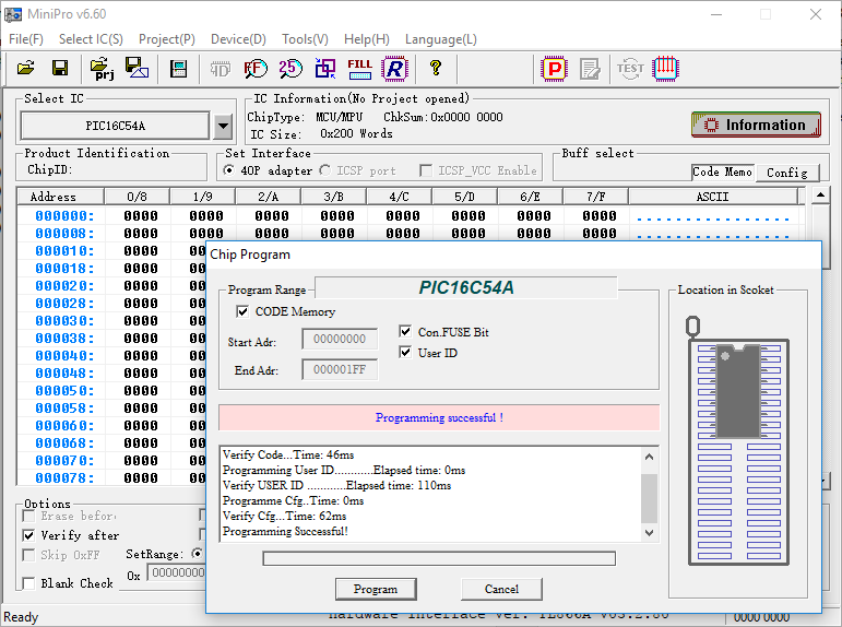
Flip every bit in the chip by filling the buffer with zeros and program it:
To expose the die to UV light and knock the trapped charge out of the floating gates, I use a vintage AT&T ES-140T EPROM eraser, but any high-output UV source will do. I insert the package into the eraser and expose it for five minutes.
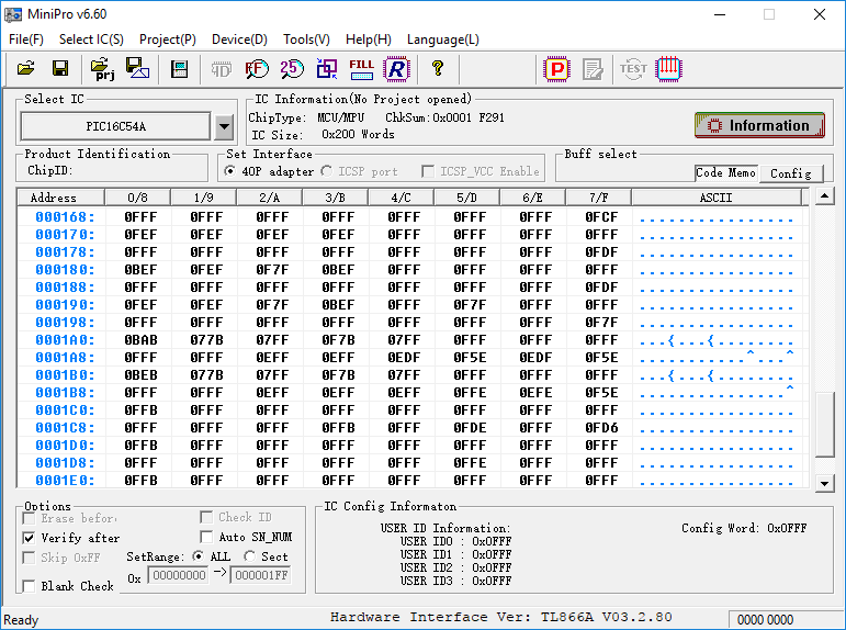
Sticking the exposed sample back in the reader reveals that most of the bits have been reset with a few stragglers remaining. Rereading the chip l also likely shows that some of the bits have flipped again. These are floating gates hovering at the discernable threshold of charge.
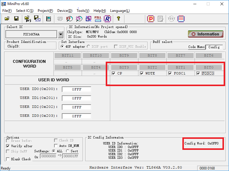
Exposing the die for an additional 10 minutes fully resets the chip to a virgin, unprogrammed state. I flip over to the chip-configuration section, which includes various hardware flags and timer settings such as the Code Protect (CP) flag. I toggle them all on and note the value of the Config Word change. Since the default state is logic high, setting these flags actually clears bits.
After programming these flags and reading back the contents, I find that the output has changed and is returning a (simplistic) hash of its contents. To complete the test, I place the die back in the EPROM eraser and expose it for the same 15 minutes I used to erase the program contents the first time.
Reading back the contents once again, I find ...that nothing has happened! All of the configuration bits are still set and the contents are still hashed. Why is this? Either the floating-gate transistors are obstructed by something and less UV light is reaching the floating gates, a different fusible technology is being used, I’ve just hit an actual invasive attack mitigation, or a combination of all three.
This is actually a good thing, as it confirms that the configuration flags are stored in a separate structure of the chip. If the configuration flags were reset in the same time period as the floating gates, it might indicate that they are collocated with the main storage area, making manual masking extremely difficult if not impossible.
I test the first hypothesis by further exposing the chip for an additional half hour. To my great relief, all of the configuration bits are reset including the CP. This implies that these transistors are imperfectly shielded by a countermeasure; some UV light is still bleeding into the floating gate, but at a reduced rate. Ican further test by pulling a trick out of bunnie’s sleeve and try to shine more light under the shielding by holding the chip at an angle relative to the light source, a method made possible initially milling out a chamfered pocket in the package and mounting it at an angle in the EPROM eraser. After exposing the package for only 15 minutes I verify that the shielded configuration flags have been reset.
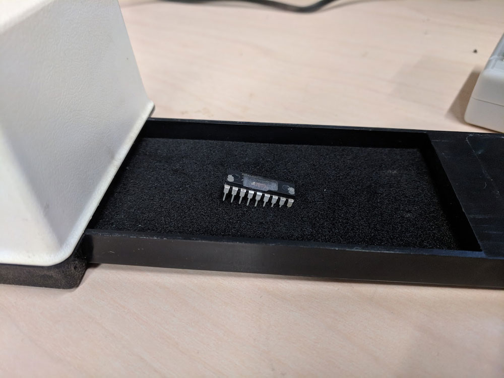
With decapsulation and UV-erasure characterization done, the only thing left to do is to shield the main floating-gate array from the UV light by manually masking off the area of the die with a non-conductive, UV-opaque material. The easiest and most forgiving of which is simple nail polish.
Using a steadied hand and a needle tip covered in a bit of nail polish, I carefully cover the gate array under a microscope.
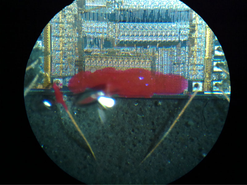
I don’t worry too much about making a sloppy mistake. As long as I don’t nick the bond wires I can soak the entire package in acetone to dissolve the nail polish and try again. I verify that I can apply a sufficiently well-defined mask by programming the microcontroller with my test pattern and resetting the configuration bits. If so inclined, I could also use this to narrow down the location of the relevant configuration fuses by selectively masking off more and more portions of the die. After this, I am ready to apply what I have learned with these tests to a locked chip and extract its firmware.
While this approach works for many microcontrollers, more security-focused devices such as SIM cards, Trusted Platform Modules (TPMs), hardware security modules ( HSMs) and other applications where system integrity is paramount, employ hardened chipsets that mitigate these and other invasive attacks. Let’s take a look at one such device, the Yubico YK4 Nano.
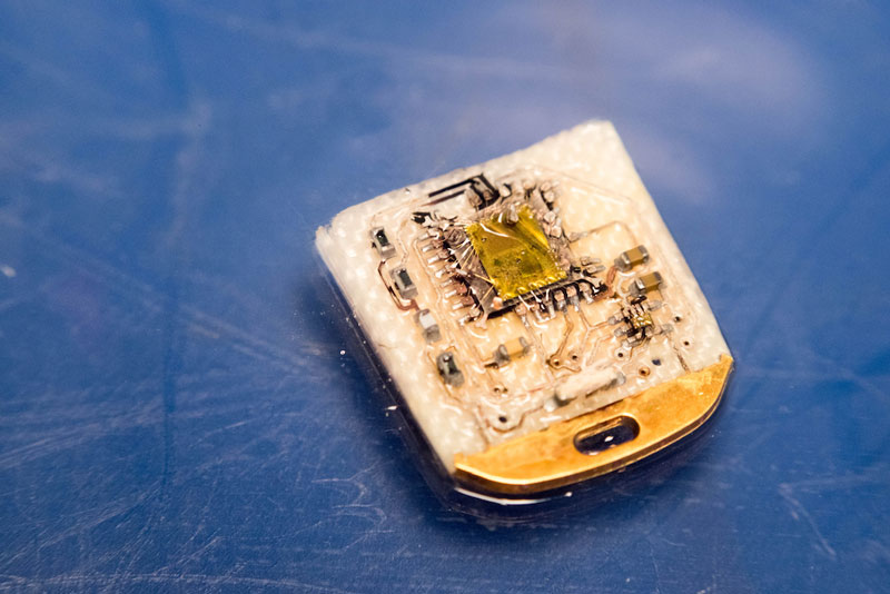
Decapsulating the YK4 and sticking it under an optical microscope reveals, well, not a whole lot. Pretty much every active part of the die apart from the bond pads is shielded by a metal layer that prevents the kind of visual inspection and simple UV tampering I described earlier.
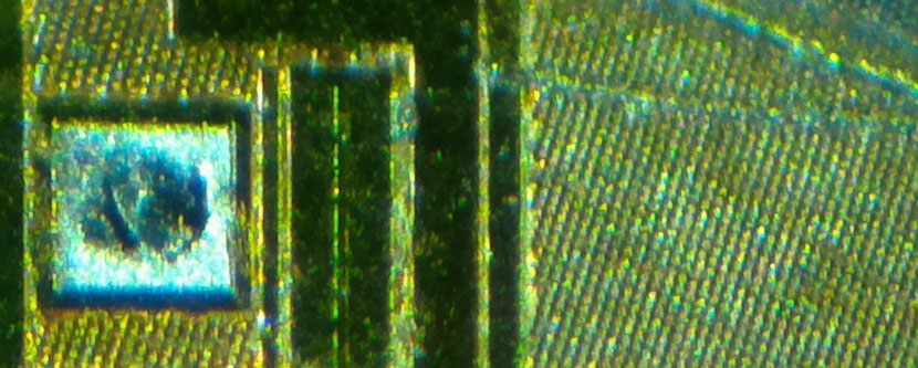
One would have to de-process the device further using more exotic (and dangerous) acids or by wet lapping to reveal the true structure hidden underneath. These are destructive processes that render the circuit non-functional.
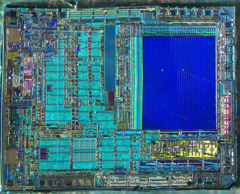
That’s not to say these types of defenses can’t be bypassed, but getting around such protections usually requires significant investment. Other types of mitigations focus on the detection of decapsulation by placing light sensors on the die itself to detect when the chips powers up after the molding compound has been removed. SIM cards often include an active mesh layer that can detect when a single trace has been cut.
If you found this interesting and want to learn more about IC security, individual feature identification and decapsulation methods, there is no better free resource than the siliconpr0n wiki. If you would like to learn more, Texplained offers a very technical training course on everything I covered here as well as on reverse engineering the implemented logic and extracting encrypted ROMs by hijacking internal circuitry.